Research
Research fields
Our research focuses on atomic-scale characterization, design, and synthesis as well as the properties of advanced materials including 2D materials, carbon materials, and soft matter by means of aberration-corrected transmission electron microscopy and spectroscopy. In situ experiments at both the atomic and nano scales are implemented for our study.
Advanced TEM Characterization
Atomic-Scale Defects Study
In Situ TEM Characterization: mechanical, thermal, and electrical experiments
In Situ Gas/Liquid Phase TEM Experiments
Research highlights
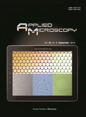
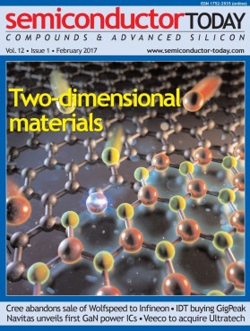
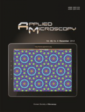
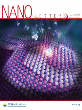
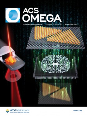
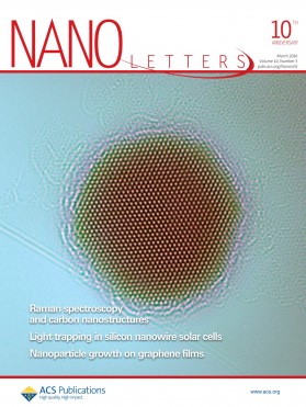
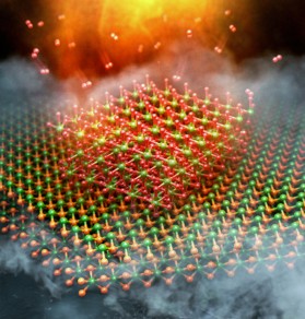
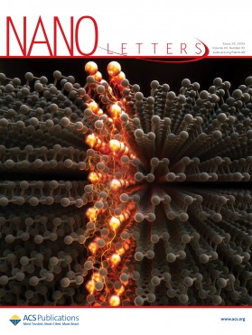
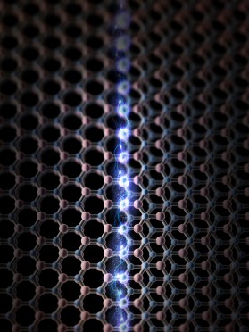
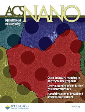
Journal covers & artworks
-
Antiphase boundaires as faceted metallic wires in two-dimensional transition metal dichalcogenides
-
Hole defects on 2D materials formed by electron beam irradiation: toward nanopore devices
-
Atomic Scale Study on Growth and Heteroepitaxy of ZnO Monolayer on Graphene
-
Atomic resolution imaging of rotated bilayer graphene sheets using a low kV aberration- corrected TEM
-
Quantitative Evaluation of Dislocation Density in Epitaxial GaAs Layer on Si Using Transmission Electron Microscopy
-
Double-Spiral Hexagonal Boron Nitride and Shear Strained Coalescence Boundary
-
In situ STEM study of MoS2 formation on graphene with deep-learning framework
-
Direct Imaging of Soft−Hard Interfaces Enabled by Graphene
-
van der Waals epitaxial formation of atomic layered α-MoO3 on MoS2 by oxidation
-
Anisotropic Angstrom-Wide Conductive Channels in Black Phosphorous by Top-down Cu Intercalation
-
One-dimensional hexagonal boron nitride conducting channel
-
Atomic-scale dynamics of triangular hole growth in monolayer hexagonal boron nitride under electron irradiation
-
Grain Boundary Mapping in Polycrystalline Graphene

